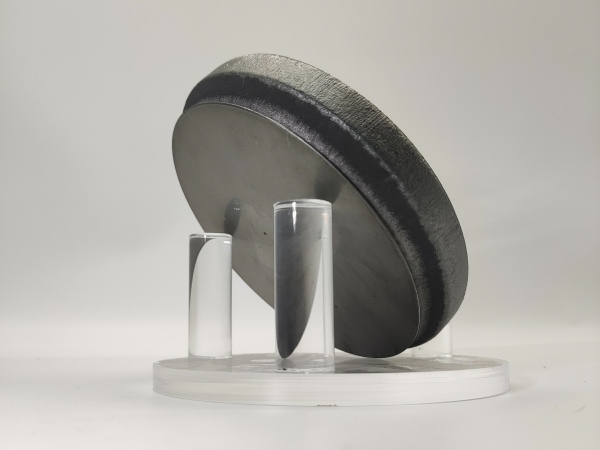
CVD can only produce a 3C-SiC seed film tens of micrometers thick, and its growth temperature is locked below 1350 °C by the silicon substrate—silicon melts at high temperature. Sublimation Epitaxy (SE) raises the growth temperature to 1600–1800 °C and is currently the most promising route to bulk 3C-SiC substrates. But SE cannot use the 3C-SiC/Si composite wafer directly; a seed-transfer-stack process must first be completed. This article explains the full CVD + SE bulk-substrate path.
1. The Seed-Transfer Stack: A Precondition for High-Temperature Growth
The as-grown CVD sample consists of a silicon substrate plus a 20–50 μm 3C-SiC film. Silicon cannot withstand SE temperatures above 1600 °C, so it must be removed completely:
1. A mixed wet etchant of HF + HNO₃ + H₂O chemically etches away the silicon substrate entirely, yielding a freestanding 3C-SiC film;
2. The side facing the original Si interface is densely defective, while the growth-front surface has excellent crystal quality and serves as the growth plane for the later bulk growth;
3. A carbon-glue layer is deposited on the defect-rich backside;
4. The film is bonded to a poly-/single-crystal SiC carrier, forming the "3C-SiC film–carbon glue–SiC carrier" seed stack, which is loaded into the PVT growth chamber.

 Fig. 1 Schematic of the seed-transfer stack.
Process challenge: the CVD-grown 3C-SiC film carries residual stress, and the wafer bow carries over to the freestanding film. Uniform pressure must be applied during bonding to suppress bending as much as possible. Seed quality directly sets the upper limit on bulk-substrate quality.
2. The SE Growth Window: A Parameter System Entirely Different from 4H-SiC Bulk Growth
The SE apparatus is adapted from the commercial hexagonal-SiC PVT crucible system, but 3C-SiC growth conditions differ greatly from
4H-SiC bulk growth. To stably maintain the cubic phase and avoid 4H/6H hexagonal polytype inclusions, the following parameter window must be strictly met:
| Parameter |
Typical window |
| Growth temperature |
1600 – 1800 °C |
| Axial temperature gradient |
14 – 19 K/mm |
| Source–seed gap |
0.5 – 1 mm |
| Chamber pressure |
10⁻³ – 10⁻² mbar (high vacuum) |
| SiC₂ vapor supersaturation |
> 0.4 |
| Vapor composition |
Si-rich; metallic tantalum (Ta) foil placed as a carbon getter to adjust the Si/C ratio |
Full process flow: first hold at 1100 °C under vacuum for 12 h to clean the chamber, then ramp up rapidly at 20 K/min to the growth temperature. Growth rate scales approximately linearly with crucible-top temperature; at 1750 °C it can reach about 240 μm/h, enabling high-speed thickening to hundreds of micrometers.

Fig. 2 Cross-section of the SE (ESE/CS-PVT) growth apparatus and seed stack. (a) Inductively heated PVT chamber: a graphite crucible inside a quartz tube, with tantalum (Ta) foil at the bottom as a carbon getter, a SiC source plate above it, a graphite spacer setting the 0.5–1 mm short gap, and the seed stack on top; (b) Seed preparation: the CVD 3C-SiC/Si is wet-etched to freestanding film and its backside is bonded with carbon glue to a SiC carrier.
It must be stressed that during SiC sublimation, SiC₂ is the rate-limiting vapor species; sufficient supersaturation must be maintained to stably obtain cubic 3C-SiC, otherwise 4H/6H hexagonal inclusions readily nucleate.
3. Defect Inheritance and Evolution in the SE Bulk Substrate
Sublimation epitaxy cannot remove defects already carried by the seed; some defects replicate directly into the new bulk layer. The paper systematically studies three key defect types:
3.1 Pyramidal Protrusion Defect: An Inherited, Fatal Defect
The four-sided pyramidal defect originates at the Si/3C-SiC interface of the CVD seed and consists of a polycrystalline core wrapped by four {111} planes. Statistics show that neither changing the SE growth rate nor increasing SE thickness eliminates the protrusion: as long as a protrusion exists in the CVD seed, it propagates into the bulk layer.
The product implication is clear: for a high-quality bulk substrate, protrusion density must be pushed low at the CVD seed stage; the SE stage cannot "repair" upstream defects.
3.2 Stacking Faults (SF): High Temperature Favors Closure
In the transition from CVD seed to SE layer, SF density rises briefly; as SE thickening continues, once total thickness reaches about 200 μm, SF density falls again, even below the original CVD seed level.
Data show that growth temperature, more than growth rate, dominates SF closure—higher temperature lets SFs terminate and close on their own; at equal thickness, a lower growth rate also further reduces SF density. This matches the CVD rule that slower growth gives better quality.
3.3 Film Internal Stress: Evidence from Raman Spectroscopy
Stress is characterized by the Raman TO mode (stress-free 3C-SiC peak at 797 cm⁻¹): a shift to higher wavenumber means compressive stress, a shift to lower wavenumber means tensile stress. The SE bulk sample remains in tensile stress, but as bulk thickness grows the tensile stress is clearly relieved—better than the original CVD film. Thus thick SE growth itself is a "release" of residual stress.
4. Current Lab Progress and Three Commercial Bottlenecks
In a 2-inch chamber, a bulk 3C-SiC single-crystal layer of 10.5 cm² area and 570 μm thickness has been grown; literature also reports an 850 μm-thick, 1-inch sample. Reaching a commercial substrate still faces three engineering challenges:
1. Large seeds limited by cracking and warpage: the area of a freestanding CVD film is hard to scale, directly capping bulk-substrate size;
2. Inheritance of pyramidal protrusions: it demands extreme upstream CVD template quality; SE cannot backstop it;
3. Hard cubic-phase stabilization: keeping pure 3C-SiC and suppressing hexagonal nucleation during high-temperature growth has a narrow process window.

Fig. 3 Cubic-phase purity and crystal-quality characterization of bulk 3C-SiC. (a) Raman spectrum (TO peak at about 797–798 cm⁻¹; peak shift reflects residual stress: higher wavenumber = compressive, lower wavenumber = tensile); (b) X-ray rocking curve (FWHM about 65.6 arcsec, assessing single-crystal quality).
5. Product Logic of the CVD + SE Combination
The division of labor across the technology chain is clear:
CVD responsibility: use large-size silicon production lines to prepare a low-cost 3C-SiC seed template, with front-end defect control (low voids, low APD, low protrusions);
SE responsibility: high-temperature, high-rate thickening to build the bulk 3C-SiC substrate, using high temperature to promote SF closure and stress release. |
Using a clean, low-rate CVD process to obtain a low-defect seed, then transferring to SE for high-temperature thick growth, combines their strengths and is currently the most feasible route to bulk 3C-SiC. The paper observes no new negative crystal-quality issue introduced by SE itself—high-temperature SE even further reduces stacking faults.

Fig. 4 Overall CVD + SE process-route diagram: Si substrate → CVD buffer layer + thick film (low-defect seed) → wet Si removal · seed transfer → SE 1600–1800 °C high-temperature bulk thickening → slicing and polishing to the bulk 3C-SiC substrate; CVD handles front-end defect control, SE handles high-temperature thickening, SF closure, and stress release.
| Summary: SE opens the path to bulk 3C-SiC substrates, but SE is not a standalone process; its performance ceiling is set by the upstream CVD seed template. Seed-transfer process, inherited protrusions, large-wafer fabrication, and cubic-phase stabilization are the four core engineering problems to solve before commercialization. For a substrate buyer evaluating a 3C-SiC supplier, both its CVD seed-quality control and SE bulk-growth process window must be examined—neither capability is dispensable. |